I’m investigating the possibility of adding a PoE splitter inside my Reform.
My idea is to power the machine with USB-C when nothing else is connected, and when the ethernet port is connected to a powered hub, let the splitter supply power instead - and free up the USB-C port for serial communication duties.
My concern is, because I’m a klutz, I will almost certainly connect a powered hub AND a USB-C power supply at the same time some day. And when that happens, I want to make sure no damage will ensue.
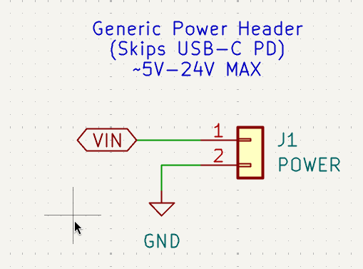
In the USB-C schematic, I see this:
This strongly suggest that I can plop any old voltage between 5V and 24V on J1 and this will disable the TPS25730D USB-C PD controller.
And in the TPD25730D datasheet, I see this:
8.3.3.1 TPS25730D Internal Sink Path
The TPS25730D has internal controls for internal FETs (GATE_VSYS and GATE_VBUS as shown in Figure 8-12) that require that VBUS_IN be above VVBUS_UVLO before being able to enable the sink path. Figure 8-12 shows a diagram of the sink path. When a sink path is enabled, the circuitry includes a slew rate control loop to ensure that external switches do not turn on too quickly (SS). The TPS25730D senses the PPHV and VBUS voltages to control the gate voltages to enable or disable the FETs.
So I’m pretty sure this will safely disable PPHV if I plug a USB-C power supply AFTER I supply power through J1. My questions is this:
-
What happens if I connect the USB-C power supply first, then I supply voltage on J1? Does it disable PPHV too or does it go ka-boom?
-
What happens if I supply voltage on J1, then connect the USB-C power supply (nothing happens), then I disconnect J1: will USB-C take over to supply power?
Another question:
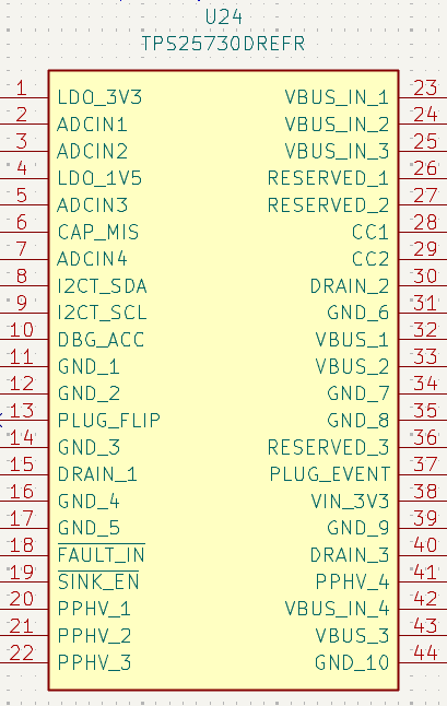
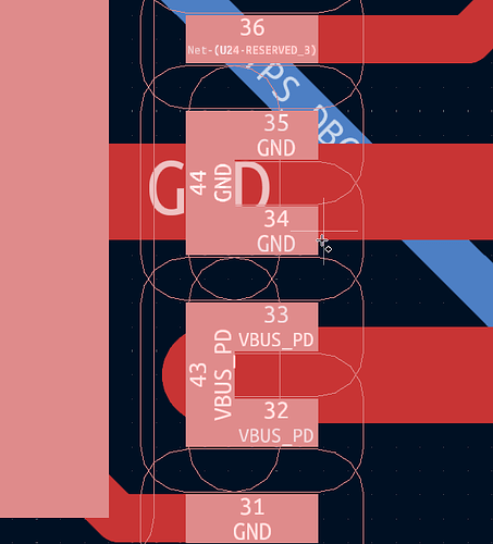
The schematic shows a TPS25730D in a 44-pin package:
But the TI datasheet only lists a 38-pin package for the -D variant of the chip. How come?
And finally, I think I found a couple problems in the schematic:
1/ The ADCIN1 divider yields a very suspicous ratio of 2.26 ÷ (198 ÷ 2.26) = 0.02579596. If you look in the table in the datasheet, that’s right at the boundary between decoded value 0 and 1:
In fact, strictly-speaking, with ideal resistors, it decodes as 1, which would set Vmin to 9V rather than 5V, contradicting the mention of 5V-24V next to the J1 header.
In contrast, the other ADCIN dividers’ ratios are:
TPS_ADCIN2 = 191 ÷ (9.31 ÷ 191) = 0.953522041
TPS_ADCIN3 = 38.3 ÷ (162 + 38.3) = 0.19121318
TPS_ADCIN4 = 9.53 ÷ (191 + 9.53) = 0.047524061
which sit squarely in the middle of the 7, 3 and 5 decoded values’ ratio ranges respectively - which is what someone who designed those dividers to hit the correct decoded values reliably would aim for.
So I think there’s a mistake in the ADCIN1 resistor values. But it’s definitely not a showstopper.
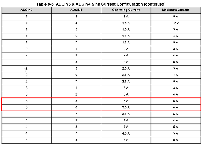
2/ ADCIN3 / 4 decode as 3 / 5. That combination doesn’t exist in the table:
I guess the chip is happy to run with an invalid current configuration - probably uses the next valid one ![]()


